Over the past two months, several sources have begun seeing Pascal GPU testing parts sent from China and Taiwan to India for testing. More recently, however, some actual Pascal-based GPU units have been shipping over the course of February and are on track to make a splash at Nvidia’s 2016 GPU Technology Conference next month.
Zauba is an India-based import and export database that allows corporate clients to track and access daily import and export shipment records to and from different countries and regions, discover new markets and gain new insights into international trade and new market opportunities.
As we wrote in February, at least four Pascal-based GPUs have been shipped from TSMC manufacturing facilities in Taiwan to Nvidia’s testing and validation facilities in India. All four models contain the same serial number prefix beginning with “699.” The four models are the 699-2H403-0201-500, 699-1H400-0000-100, 699-1G411-0000-000, and the 699-12914-0071-100.
According to the Zauba database, the most recent shipment for the 699-2H403-0201-500 was February 5, 2016, originating from China with a value of $608 USD per unit. The most recent shipment for the 699-1H400-0000-100 was December 16, 2015, originating from China with a value of $668 USD per unit. The most recent shipment for the 699-1G411-0000-000 was February 26, 2016, originating from China with a fluctuating value between $606 and $751 USD per unit. The most recent shipment for the 699-12914-0071-100 was February 4, 2016, originating from China with a value of $810 USD per unit.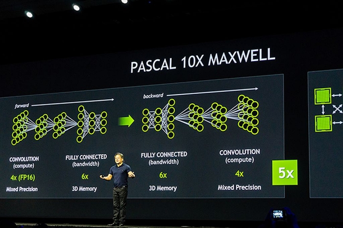
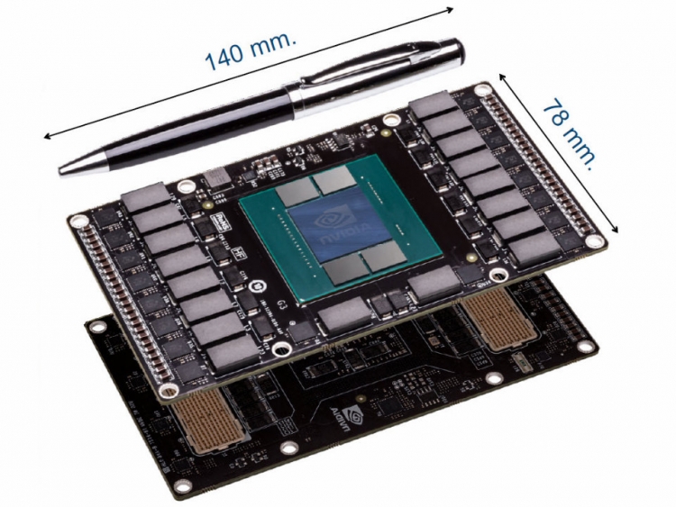
Image credit: VR-Zone
TweakTown senior GPU editor Anthony Garreffa notes that the higher-priced 699-1G411-0000-000 and 699-12914-0071-100 units could very well be the successors to the Maxwell-based Geforce GTX 980 Ti and the Geforce GTX Titan X, both based on the flagship 28-nanometer GM200 GPU. These chips are expected to come with an impressive 16GB and 32GB of High Bandwidth Memory 2 (HBM2) VRAM achieved using 4-Hi and 8-Hi stacks.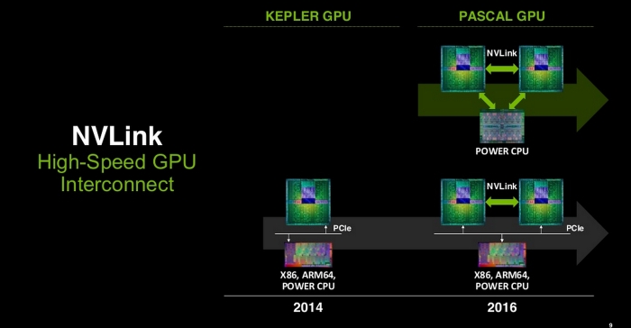
Image credit: WCCFTech
The flagship GP100 (“Geforce Pascal 100”) GPU will be the successor to the GM200 (“Geforce Maxwell 200”) GPU and features up to twice the performance-per-watt of its predecessor. Nvidia’s GP100 will contain a total of 17 billion transistors, over twice the number found in the GM200. It will also feature Nvidia NVLINK, a new proprietary ultra-high speed interconnect technology exclusively for Nvidia Geforce GPUs that will enable communication between CPU and GPU, and between GPUs at data rates between 80GB/s and 200GB/s.
The company is hosting its annual GPU Technology Conference from April 4th to 7th in San Jose, California, and we expect this will be a prime opportunity for CEO Jen-Hsun Huang and senior Nvidia graphics architects to show the international GPGPU developer community and the rest of the world the incredible quantum leap in performance that Pascal will offer compared to 28-nanometer Maxwell chips.
We will be at GTC 2016 this year and look forward to sharing more concrete details on Pascal part numbers, retail pricing, and last but not least, the SKU naming scheme that Pascal will adopt as coming after the Maxwell-based “Geforce GTX 900 Series.”