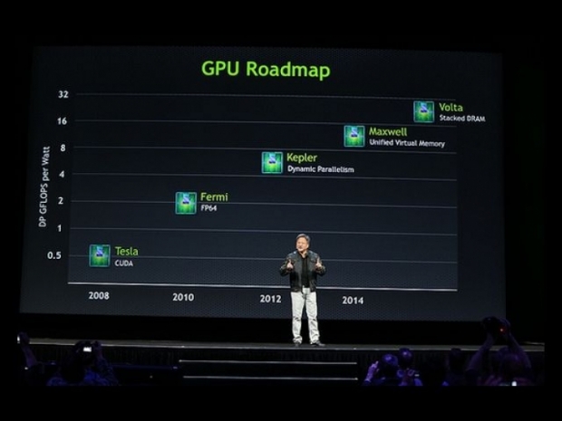
For those who came in late, Volta was supposed to be a 10nm process, but that proved a little too tricky. The last rumour had Nvidia sticking with TSMC’s 16nm tech so it could keep to its roadmap and get Volta cards on the shelves before the sun turns into a red giant.
TSMC has, though announced another stop-gap measure which it's calling 12nm which is its existing 16nm design with wind spoilers and “go faster stripes”. TSMC claims to have pimped up density, performance and energy efficiency but actual 12nm transistors are about as likely as Jeremy Corbyn being British Prime Minister.
According to PC Games Mag, Nvidia will now be taking TSMC’s updated 16nm design for its Volta GPUs to augment the new architecture’s own performance and power improvements with the extra bump of a shrunken lithography.
Nvidia’s Volta GPU tech will probably be shown off at the Graphics Technology Conference in May so it is ready for next year. Oak Ridge National Laboratory’s new Summit supercomputer, which was initially designed to launch with Volta GPUs this year, has been pushed back to 2018 probably because of this issue.
Rumours are that Volta GPUs will have either GDDR6 or HBM2 at different levels of card. The GDDR6 has a memory speed of 16Gbps.
However, this year we will see refreshed Pascal GPUs and probably a new Titan. Which might give AMD a chance to put its foot in the door and claw back a bit of market space.


