While it did not provide a lot of details, Samsung claims that the 10nm LPP will bring up to 10 percent higher performance or 15 percent lower power consumption when compared to the 10nm LPE. The company also claims that this 2nd generation 10nm FinFET process technology also reduces the time from development to mass production and provides significantly higher manufacturing yield.
According to Ryan Lee, VP of Foundry Marketing at Samsung Electronics, the company will be able to better serve its customers through the migration from 10nm LPE to 10nm LPP with improved performance and higher initial yield and will continue to work on the evolution of 10nm technology down to 8nm LPP process.
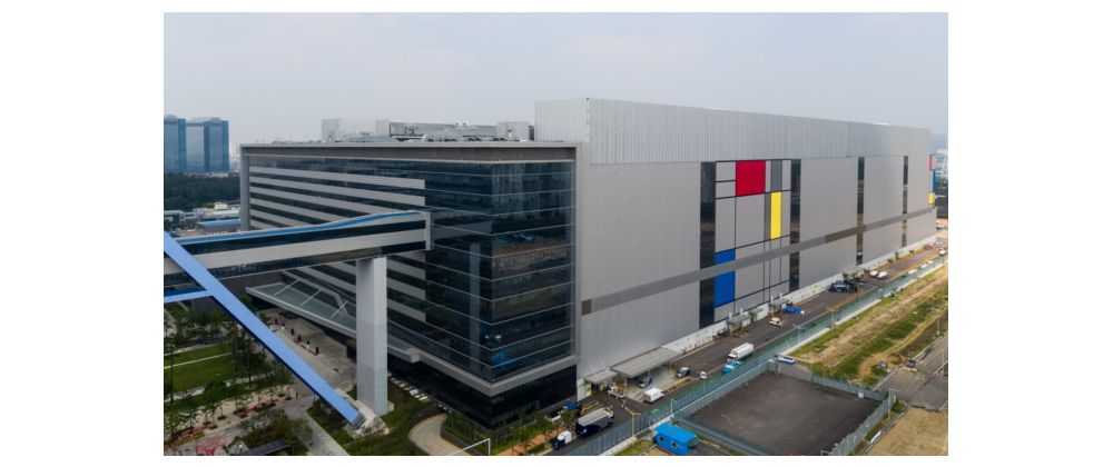
Samsung also took the opportunity to announce its newest S3 manufacturing line at Hwaseong, Korea, which is ready for production of 10nm and below as well as the future 7nm FinFET EUV (Extreme Ultra Violet) manufacturing process.


