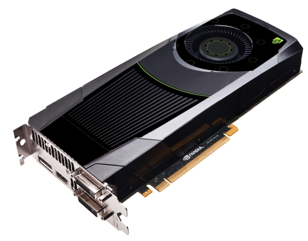
Nvidia has finally launched its GTX 680 graphics card, probably one of the most anticipated Nvidia cards in recent years. Based on TSMC made 28nm Kepler GK104 GPU, the new GTX 680 features 1536 CUDA cores and brings quite a few new features.
The new 28nm GK104 Kepler GPU behind the GTX 680 card has a die size of 294mm2 and features 3.54 billion transistors. Those 1536 CUDA cores are orginized in four graphics processing clusters or GPCs that feature shared L2 cache, single raster engine each and two streaming multiprocessors that are now called SMXs. Each SMX has its own PolyMorph Engine 2.0, some L1, texture and instruction cache as well as 192 CUDA cores. The GPU also features 32 ROPs and 128 texture units.
When we heard first rumours regarding GK104, we were quite surprised that Nvidia has started to use sentences like power efficiency and performance per Watt, but now it looks like the GK104 is just about that. With a TDP of 195W, which leads to 6+6-pin configuration on the PCB, Nvidia's GTX 680 is certainly challenging AMD on its home turf, and doing it impressively if we may add.
The card ended up clocked at 1006MHz for base clock and 1500MHz (6.0GHz effective) for 2GB of GDDR5 memory. The new feature called GPU Boost that takes the clock to somewhere around 1058MHz in average gaming scenario. We did say "to somewhere around" as this clock is actually sometimes higher, but we will leave detailed explanations for a different article, or our review.
In addition to GPU Boost dynamic overclocking, the new Nvidia GTX 680 also brings new TXAA and FXAA antialiasing algorithms, new adaptive V-sync, multi-diplay support with a total of four displays and 3D Vision Surround on a single card, new NVENC encoder as well as new "bindless textures" feature. Since explaining each of these in this article would make it way too long, we'll leave features for a different one.
The reviews around the net are very positive as the new card it simply ends up faster than AMD's Radeon HD 7970. The best part for Nvidia is that it doesn't just end up faster, but also brings multiple new features, and does it with lower power consumption. To sweeten the deal, Nvidia did a last minute (or last two days) price adjustment, launching its new card at US $499 ex. tax, which makes it US $50 cheaper than the HD 7970.
Most complaints were aimed at limited, and now complicated, overclocking potential due to GPU Boost as currently, there is no way to disable it. This will certainly upset many enthusiasts and overclockers as currently you can only set the GPU to +549MHz clock offset that the dynamic overclocking algorith will try to respect.
Our friend Wizzard from Techpower did quite a piece on this topic, and according to his results, maximum stable one is set at 1147MHz for the GPU, 1200MHz for Boost and 1833MHz (7332MHz effective) for memory. We must compliment Nvidia regarding the memory situation as it appears that they did quite a good job on that part.
The ball is now in AMD's hands as currently Nvidia has the upper hand and GTX 680 certainly sounds like a great deal.
Here are some of the review that we gathered around the net.
- Techpowerup.com
- Anandtech.com
- Hothardware.com
- Legitreviews.com
- Tweaktown.com (with its early we-don't-like Nvidia review)
- Hardwarecanucks.com
- Xbitlabs.com


