Despite 50 percent more EUs from Gen 11 graphics and reaching 96 EUs and 1536 flops per clock, the GPU die size didn’t dramatically change. Without getting to any specific numbers, David confirmed that the GPU ended up being not a lot bigger.
New architecture, new transistor, and higher clocks
The GPU design team has to increase efficiency and rewrite everything on the hardware and software size, as this is a brand new design for Intel and foundation for higher performance integrated parts in the future.
The magic mix is to increase performance per square millimeter, performance per watt, and performance per flop simultaneously. The main goal was to get twice the performance of Ice lake Gen 11, which David described as a pretty daunting task.
Intel came from the ground up with a new architecture called Xe LP. The Intel design team had to work closely with the manufacturing teams in order to make this design possible.
Xe LP 96 EUs
David describes Xe Lp as a GPU with 96 Execution units and 1536 flops per clock, up to 48 bilinear texels per clock through six samples and up to 24 pixels per clock through the pixel pipes.
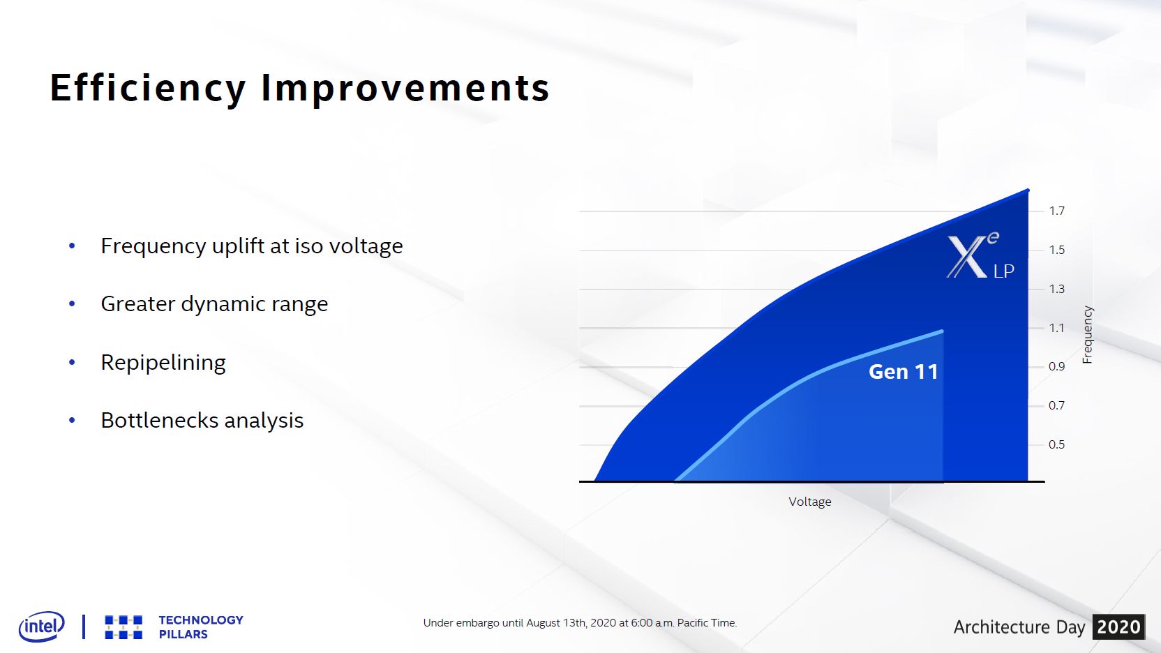
Increasing the number of Execution units from the previous Gen 11 GPU designs by 1.5 was an optimal goal to reach a 2X performance. The mix of the new transistor and new architecture helped in achieving a 2X performance goal set by design.
David also mentioned that the mix of higher GPU clock, new transistors, and the new architecture design helped to keep the TDP and GPU size at the same level, still getting a significantly faster performance.
One of the slides implicates that the new GPU might run faster than 1.7GHz, much faster than Gen 11’s 1.1 GHz maximal clock speed. David describes advantages in frequency uplift at ISO voltage, greater dynamic range, re-pipelining the GPU, as well as the bottleneck workload analysis as the extra tools that helped Intel get to the 2X performance increase.


