Index
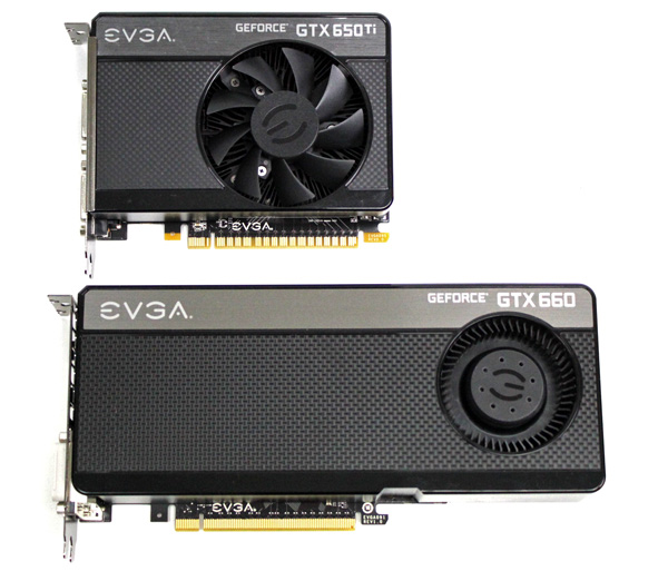
The GTX 650 Ti SSC is the shortest Kepler based card so far. It couldn’t have been made shorter because of the PCI Express connector length.
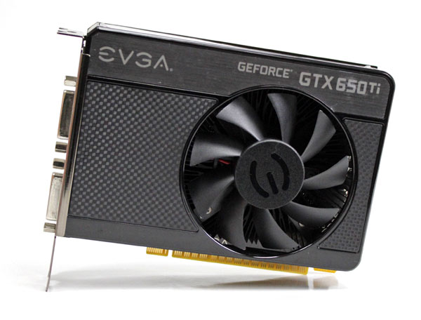
The PCB is only 14.5cm long, which is about the length of the cooler shroud.
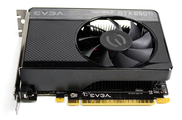
The picture below shows the GTX 660, which also uses the GK106 GPU. Its PCB is 17.3cm long while the cooler measures 24.3cm together with the shroud. The GTX 650 has a TDP of 110W, which is 30W less than the GTX 660. Nvidia allows smaller coolers, i.e. GTX 650 designs, and EVGA took them up on this offer.
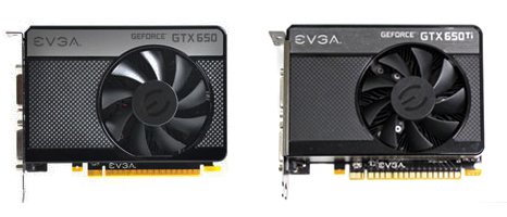
EVGA GTX 650 Ti SSC looks pretty much identical to the GTX 650 SC, or any other EVGA GTX 650 for that matter.
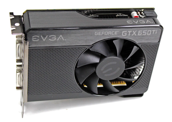
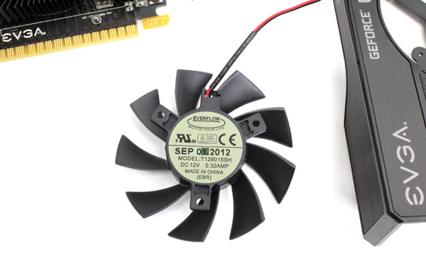
The card has dual slot cooling that relies on a single down-draft 80mm fan. The shroud isn’t completely closed up but at least has no exhausts between the fan and I/O panel, so at least some hot air will exit the case.
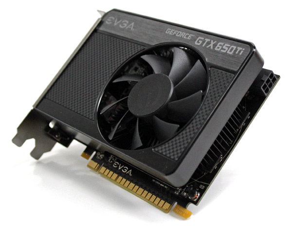
The GTX 650 Ti draws power via one 6-pin connector, just like the GTX 650, although the latter’s TDP is mere 64W.
The fan is part of the shroud. Taking off the shroud reveals a circular heatsink.
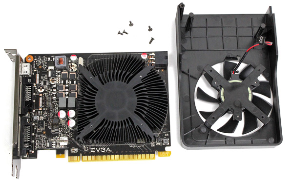
Two phases are left for the GPU while another one, towards the top of the PCB, was left for the memory.
The heatsink is one slot wide, but the fan takes up another.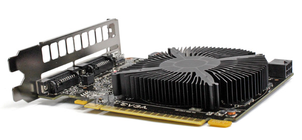
GTX 650 Ti supports triple displays straight out of the box. This is why the I/O panel has two dual link DVIs and a mini-HDMI out. EVGA threw in a DVI-to-VGA dongle as well.
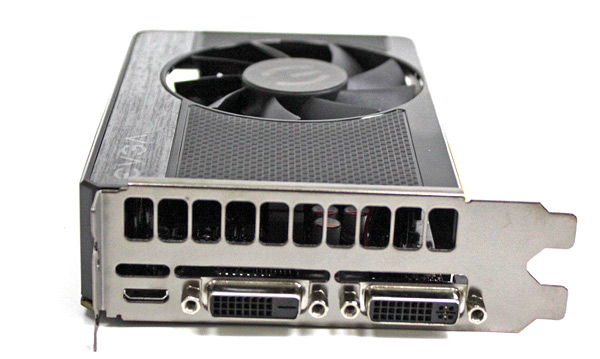
GTX 650 Ti / GTX 650 don’t have SLI connectors and SLI is not possible via PCI Express connector.
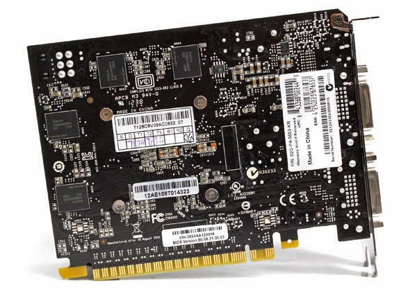
The GTX 650 Ti SSC packs 2GB of memory, evenly distributed on two sides of the PCB. The card uses Hynix memory chips (model No: H5GQ2H24AFR-R0C). The chips are specified to run at 1500MHz (6000MHz GDDR5 effectively) but GTX 650 Ti SSC’s memory runs at 1350MHz (5400MHz effectively).
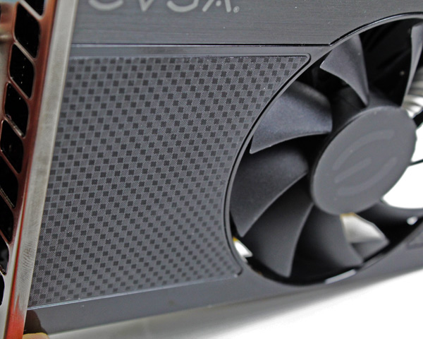
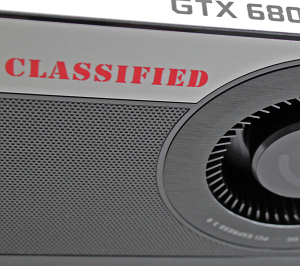
EVGA changed the texture work on the shroud and since it’s now smooth and without holes, it will not gather dust as much. While the likes of EVGA’s GTX 680 Signature 2 are visually more appealing, they’re quick to collect dust and harder to clean.
